Semiconductor Systems Integration in Jardinópolis, São Paulo
We provide specialized systems integration for the semiconductor sector, focusing on wafer fabrication automation, cleanroom robotics, and fab monitoring infrastructure. Our engineering teams deploy deterministic control logic, SCADA process visibility, and high-fidelity telemetry to ensure maximum uptime, contamination control, and unit-level traceability across complex production and fabrication environments.
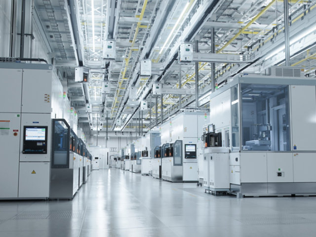
Semiconductor fabrication environments require the highest level of deterministic control and environmental stability. Integration in this vertical involves orchestrating wafer handling robotics, atmospheric control logic, and precision chemical delivery systems into a unified operational framework. Our focus centers on stabilizing the technical backbone that supports these ultra-high-precision operations, ensuring that data acquisition is reliable and process variables are maintained within sub-micron tolerances. Failure to maintain logic synchronization in a fab environment can lead to significant yield loss and hardware damage. Our methodology emphasizes the use of hardened industrial networks and secure telemetry to protect the integrity of fabrication data. By implementing intelligent cleanroom monitoring and automated wafer inspection cells, we enable operators to maintain absolute visibility over production metrics. From real-time path planning in robotics to the architecture of high-density process monitoring rooms, our systems are architected for 24/7 reliability and maintainability in ISO-rated cleanrooms. This technical rigor ensures every command is verified and every sensor packet is logged within an immutable framework suitable for quality audits and operational forensic analysis.
Providing technical integration services to industrial facilities within the Jardinópolis metropolitan area and throughout São Paulo.
Technical content for Semiconductor Systems Integration in Jardinópolis, São Paulo last validated on April 5, 2026.
Services
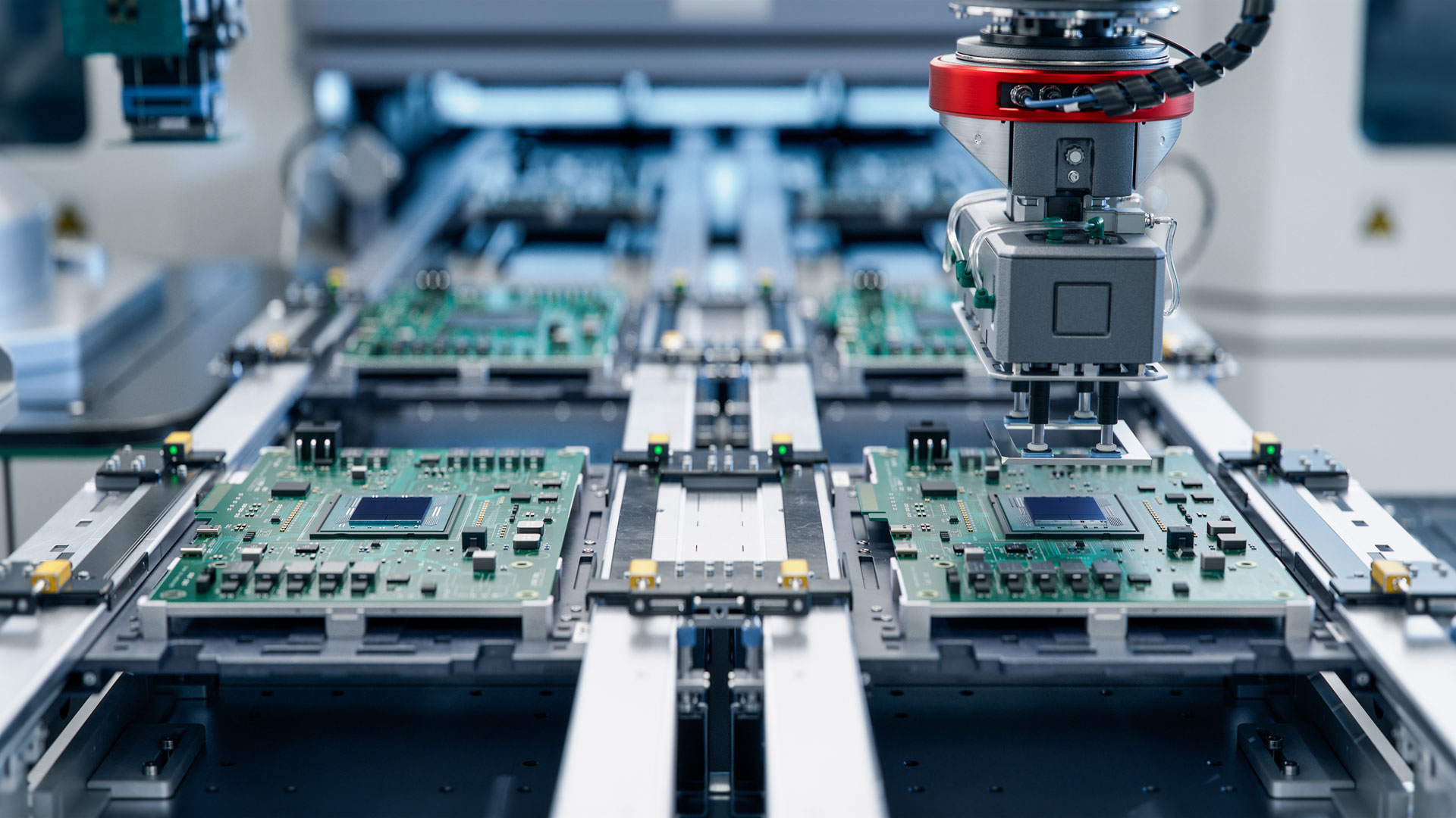
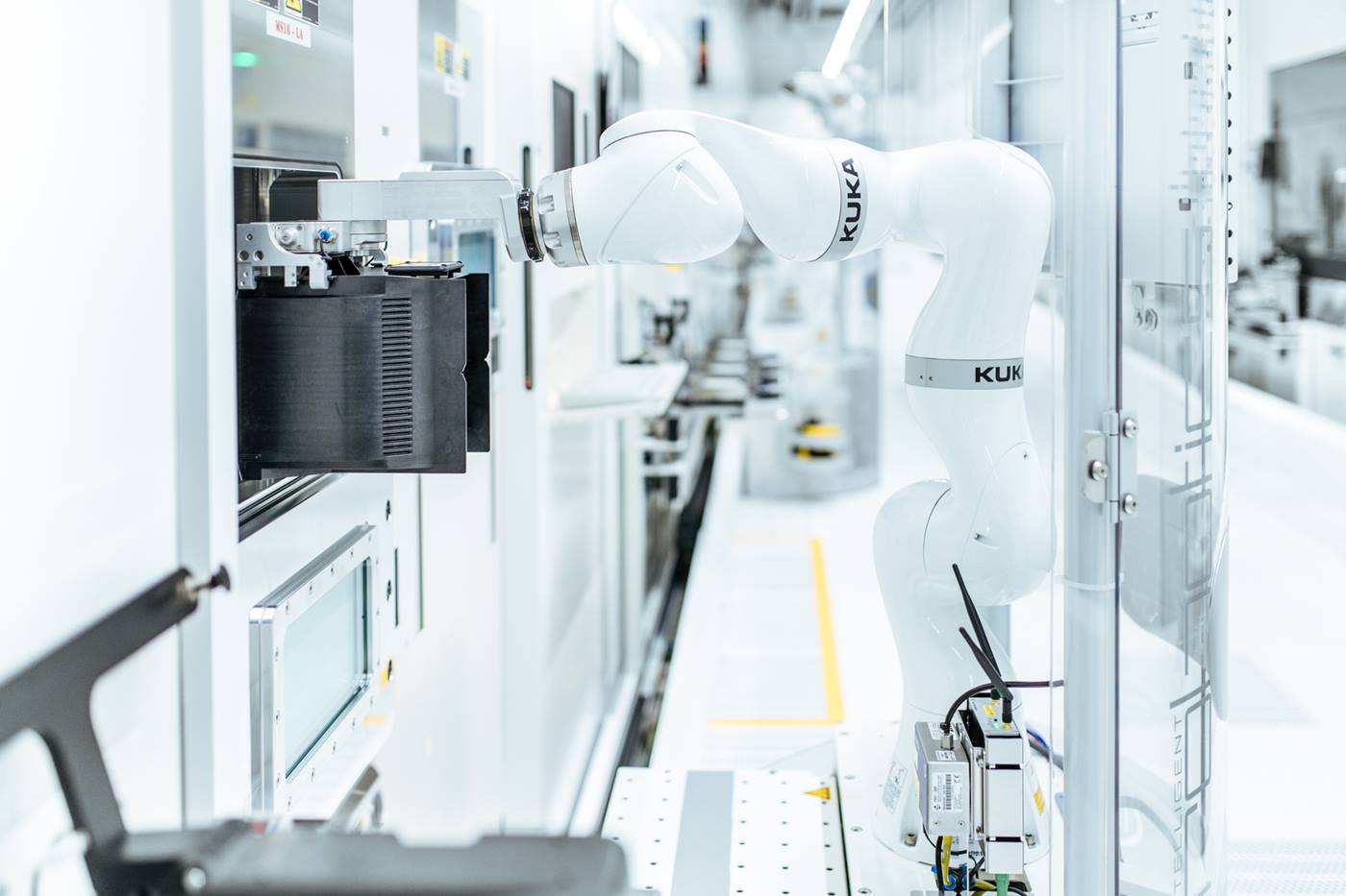
Wafer Fabrication Automation
Integration of automated production lines slaved to master PLC controllers for precise wafer processing sequences and synchronized chemical delivery.
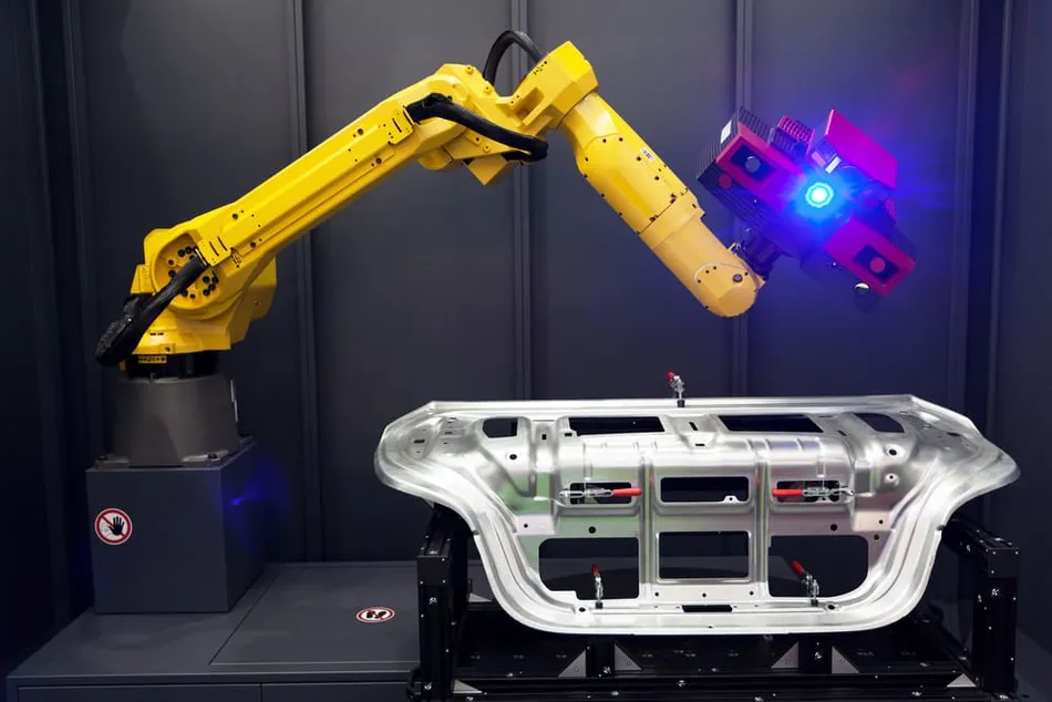
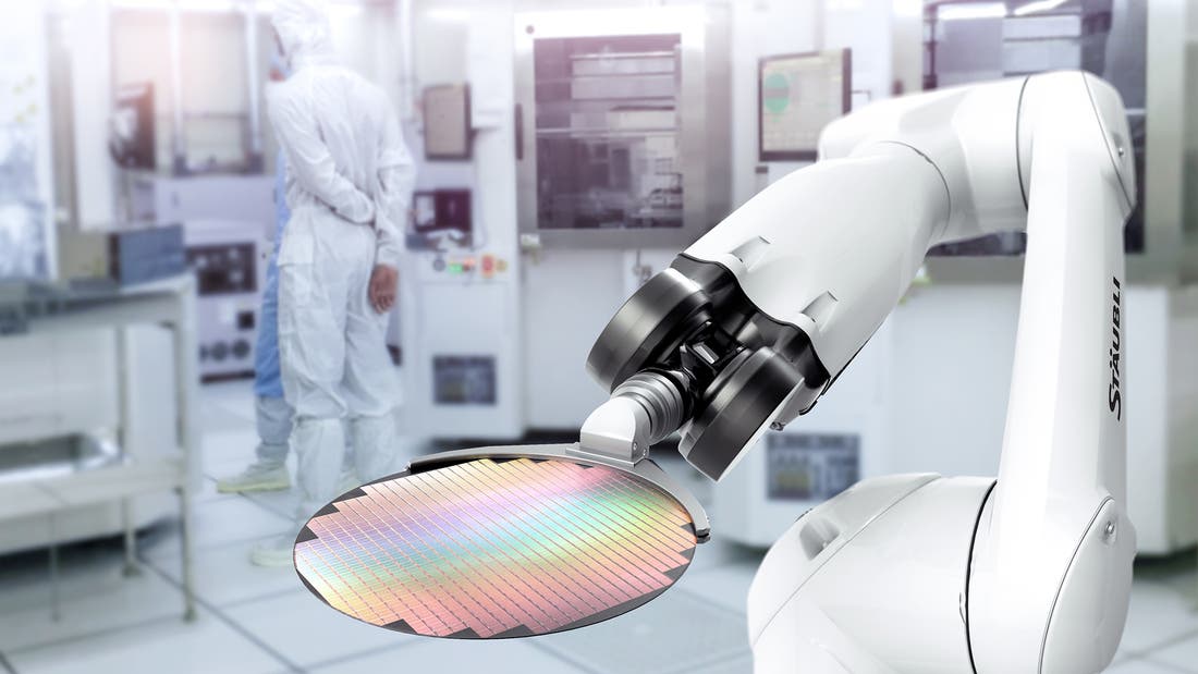
Cleanroom Robotics Integration
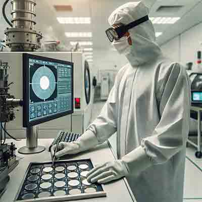
Deployment of high-speed articulated arms and vacuum end-effectors for non-contaminating wafer transfer and precision positioning in sterile environments.
Fab Monitoring Infrastructure
Architecture of centralized SCADA platforms providing real-time visibility into cleanroom air quality, pressure differentials, and chemical distribution health.
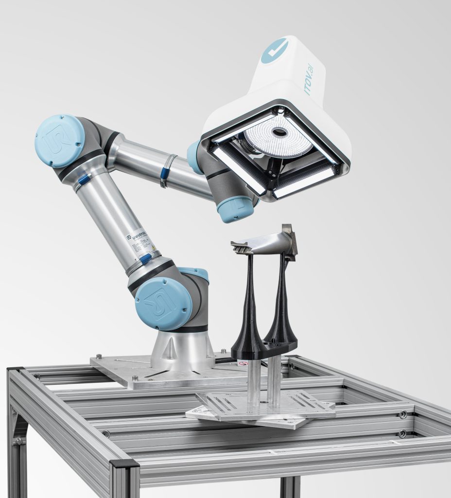
Wafer Inspection System Logic
Programming of high-speed trigger logic and high-fidelity data acquisition for automated optical inspection and real-time defect tracking.
Process Telemetry & Data Logging
Implementation of high-bandwidth industrial networks slaved to edge logging hardware for 100% process variable traceability and audit compliance.
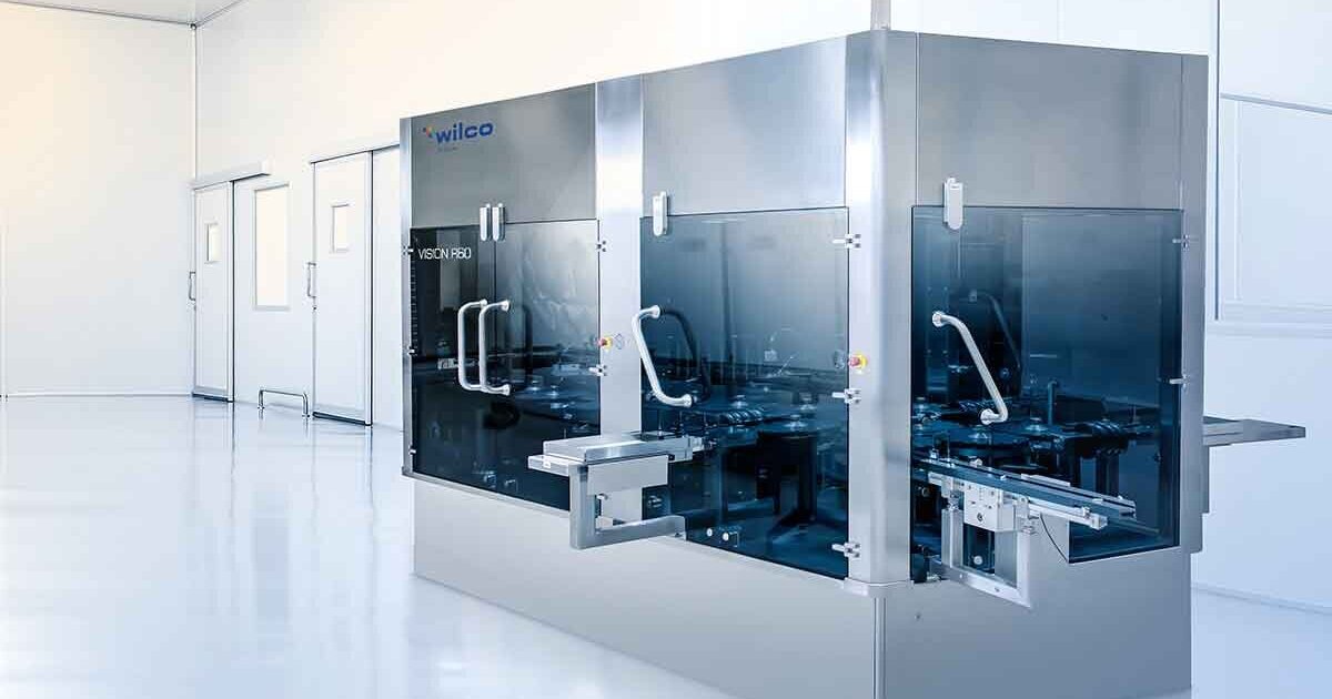
Semiconductor Test Equipment Integration
Orchestration of probe stations and thermal testing units into a unified diagnostic network for automated verification and failure analysis.
Our Process
Technical Site & Compliance Audit
Analysis of ISO cleanroom classifications, I/O magnitude, and required wafer cycle times to define specific hardware and protocol specifications.
Control Logic & Architecture Design
Engineering of a deterministic control topology and redundant controller paths slaved to navigation reliability, contamination control, and failsafe targets.
Hardware Synchronization & Integration
Physical mounting and logical pairing of field instruments, vacuum controllers, and robotic handlers via hardened industrial Ethernet and PLC interfaces.
Operational Validation & SAT
Execution of rigorous Site Acceptance Testing to verify contamination control integrity, logic interlocks, and telemetry packet accuracy under peak load.
Use Cases
Integration of a centralized monitoring hub for a wafer fab, aggregating 2000+ data points from chemical delivery systems and atmospheric sensors.
Deployment of an autonomous mobile robot fleet for wafer FOUP transport, slaved to a master fleet coordinator and plant-wide SCADA monitoring.
Modernization of a legacy wafer handling station with low-latency communication links and high-performance HMI dashboards for real-time operator visibility.
Architecture of a redundant control system for ultra-pure water filtration, ensuring continuous supply for critical semiconductor cleaning and etching stages.
Engineering of an automated optical inspection station slaved to deterministic trigger logic for real-time defect classification on a 300mm wafer line.
Technical Capabilities
- Atmospheric transfer robots utilize non-outgassing materials and sealed joint architectures to maintain ISO Class 1 cleanliness during high-speed wafer movement.
- SECS/GEM communication protocols allow for the standardized exchange of process data between fabrication equipment and factory-level monitoring systems.
- Deterministic PLC scan times are critical for managing high-speed safety-rated monitored stops in automated wafer handling cells to prevent substrate damage.
- Managed industrial switches for semiconductor facilities utilize VLAN segmentation to isolate sensitive process telemetry from high-bandwidth vision inspection traffic.
- Closed-loop PID control in cleanroom HVAC logic ensures pressure differentials are maintained within millisecond intervals to prevent particulate contamination ingress.
Semiconductor Systems Integration support
Semiconductor Systems Integration services for facilities in Jardinópolis, São Paulo, Brazil .
Semiconductor Systems Integration support
Semiconductor Systems Integration services for facilities in Jardinópolis, São Paulo, Brazil .
Semiconductor Systems Integration support
Semiconductor Systems Integration services for facilities in Jardinópolis, São Paulo, Brazil .
Semiconductor Systems Integration support
Semiconductor Systems Integration services for facilities in Jardinópolis, São Paulo, Brazil .
Semiconductor Systems Integration support
Semiconductor Systems Integration services for facilities in Jardinópolis, São Paulo, Brazil .
Semiconductor Systems Integration support
Semiconductor Systems Integration services for facilities in Jardinópolis, São Paulo, Brazil .
Semiconductor Systems Integration support
Semiconductor Systems Integration services for facilities in Jardinópolis, São Paulo, Brazil .
Semiconductor Systems Integration support
Semiconductor Systems Integration services for facilities in Jardinópolis, São Paulo, Brazil .
Semiconductor Systems Integration support
Semiconductor Systems Integration services for facilities in Jardinópolis, São Paulo, Brazil .
Frequently Asked Questions
How is contamination control maintained during the integration process?
We utilize cleanroom-certified tooling and adhere to strict gowning and material wipedown protocols to prevent particulate ingress during hardware installation and commissioning.
Can legacy fabrication equipment be integrated into modern SCADA networks?
Yes, we utilize protocol gateways and distributed I/O blocks to extract data from older tools, normalizing signals for plant-wide visibility and historian logging.
What is the primary benefit of deterministic networking in a fab?
Deterministic frameworks ensure that critical control packets, such as robot stop commands or valve triggers, receive priority, eliminating the latency that causes process failures.
How do you handle data traceability for individual wafers?
We implement unit-level tracking slaved to the control layer, ensuring that every process variable, from thermal exposure to chemical concentration, is logged against a specific wafer ID.
Quantify Your Fab Integration Requirements
Submit technical specifications for an engineering review of your wafer fabrication automation or cleanroom monitoring project.
Request Technical Audit